
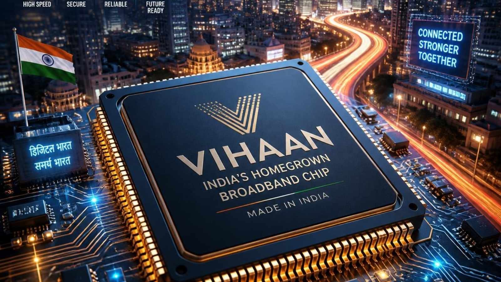
India’s Homegrown VIHAAN Broadband Chip Hits Major Silicon Milestone Ahead of 2027 Rollout
In a landmark achievement for India’s semiconductor ambitions, Chennai-based fabless startup Aheesa Digital Innovations has successfully achieved first-pass silicon success for VIHAAN—the country’s first indigenously designed broadband networking System-on-Chip (SoC). Powered by C-DAC’s homegrown 64-bit VEGA processor, the 28nm networking silicon passed initial testing on Independence Day after being taped out on Republic Day. Announced by the Ministry of Electronics and Information Technology, this breakthrough positions the VIHAAN chip for commercial production tapeout by 2027, marking a pivotal turn toward domestic chip sovereignty.
What Makes VIHAAN a Game-Changer for Fiber Broadband?
VIHAAN is purpose-built to power next-generation optical fiber access networks, Fiber-to-the-Home (FTTH) connections, and broadband customer premises equipment (CPE) across Indian households and businesses. By integrating compute functions, broadband access control, and high-speed packet routing onto a single die, the chip eliminates the need for foreign component imports in critical telecom gear.
The architecture leverages the open-standard RISC-V processor architecture, utilizing the VEGA core developed under MeitY’s Microprocessor Development Programme. By embedding a hardware root of trust, secure boot, and cryptographic acceleration engines, VIHAAN provides a sovereign security shield against firmware vulnerabilities in national broadband infrastructure. This achievement joins a rising wave of indigenous technology achievements transforming India from a technology consumer into a high-value hardware designer.
VIHAAN Technical Overview and Roadmap
| Parameter | Specification & Feature Details |
| Developer Firm | Aheesa Digital Innovations (Chennai, Tamil Nadu) |
| Processor Architecture | 64-bit VEGA Microprocessor Core (Open RISC-V) |
| Process Node | 28-nanometer (28nm) Broadband Networking SoC |
| Primary Target Applications | FTTH Routers, GPON/EPON Access, 5G Wireless CPE |
| Key Development Milestone | First-Pass Silicon Success (August 2026) |
| Mass Production Target | Production Tape-out scheduled for 2027 |
| Government Policy Support | MeitY Design Linked Incentive (DLI) Scheme |
Government Backing and the DLI Incentive Boost
The development of VIHAAN was bolstered by the government’s flagship Design Linked Incentive scheme, which provides financial support and EDA design tool access to promising semiconductor startups. Earlier this year, Aheesa secured ₹40 crore in funding led by the Tamil Nadu Emerging Sector Seed Fund (TNESSF) and private investors to accelerate chip design and testing.
Chip design accounts for nearly 50% of total value addition in the semiconductor value chain, providing massive economic margins even before domestic fabrication foundries come fully online. The milestone directly mirrors broader national mandates highlighted during recent Independence Day announcements, where PM Narendra Modi outlined expanding domestic semiconductor capabilities across design and manufacturing. Parallel growth across academic institutions and research centers continues to fuel these milestones, complementing ongoing engineering research and innovation nationwide.
Strengthening India’s Broader Semiconductor Ecosystem
Aheesa’s success is part of a larger surge across India’s fabless chip design landscape. Under the semiconductor incentive programs, over 30 chip designs have successfully taped out a
cross various global foundries, with supported startups collectively raising more than $100 million in venture capital. In addition, chip-design software tools have been distributed to over 455 organizations, including 350 academic institutions, training a skilled workforce of hardware engineers.
By replacing imported silicon from global tech giants with homegrown alternatives like VIHAAN, Indian telecom operators will soon deploy fully locally engineered networking equipment. As Aheesa moves toward its 2027 commercial production tapeout, the VIHAAN chip stands as concrete proof that India can lead in high-complexity silicon design.
